
signal integrity in pcb circuit board
Printed circuit board (PCB) manufacturers need to ensure that digital/analog signals stay uncorrupted during transmission through interconnects and can be retrieved at the receiving end without distortion. This guarantees that the device performs its intended function and also prevents the circuit board from radiating electromagnetic interference (EMI) that would impact other electronics in close proximity. Fortunately, there are some straightforward layout practices that can help with this.
A good pcb circuit board design starts with a layer stackup that includes dedicated layers for sensitive high-speed routing and adjacent reference planes in a microstrip or stripline configuration. This can help minimize the loop area on a signal line and reduce its inductance. In addition, signal return paths need to be free of obstructions and routed on an adjacent reference plane for the best signal integrity.
High-speed traces should not be positioned side-by-side as this can result in crosstalk that causes the victim signal to mimic the characteristics of the aggressor signal and interfere with its performance. This is why most high-speed traces are alternated on different layers. Assigning a ground plane to the PCB is another simple yet effective measure that can greatly improve signal integrity. This reduces the loop area on the grounding line and limits its inductance, which can cause interference and other problems.
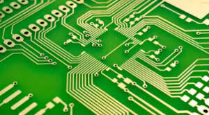
How do you ensure signal integrity in pcb circuit board?
When designing a pcb circuit board, you need to make sure that you have enough space for ICs, connectors, and passive components as well as sufficient clearance for traces. This is important because the additional distance between signals slows them down and reduces overall system speed.
The PCB’s copper traces act as transmission lines at high frequencies, and their impedance values change from one end of the trace to the other. The change in impedance is proportional to the switching frequency, and it can cause ringing or reflections that degrade the signal quality.
Historically, finding and fixing these coupling issues required significant time and specialized tools to debug a physical prototype. The good news is that today’s CAD systems include a number of signal integrity and EMI simulation tools that can detect and correct them in the virtual design phase before sending a circuit board out for manufacturing.
Having signal integrity and EMI management features built into the CAD system makes it possible for PCB designers to avoid costly delays and malfunctions by detecting and fixing signal integrity and EMI problems before the board goes through prototype testing and certification. This means that you can focus on bringing your new device to market faster. The faster you can get your product to market, the more money you can make. The quickest way to get there is by using the right pcb assembly service provider. This will ensure that your products are as reliable and powerful as they can be.