
Blind Via Holes Suitable For Fine-Pitch
With component lead pitches getting finer and smaller form factor devices starting to dominate a lot of PCB designs, there is a real need for more interconnections on the inside of the board. While there are several ways to make these connections, one of the more common is through the use of via holes. The IPC defines eight different types of vias, but we will focus on blind and buried vias here as these are the two you are most likely to encounter in your own PCB design work.
A via hole is a barrel-shaped vertical conductive connection on a multilayer PCB that can connect layers of the board to each other. There are two types of vias, blind and buried, and a third type that goes all the way through the board (a through-hole).
These vias can be plated either before or after the lamination process and can be drilled either before or during the etching process. The plated vias will be filled with copper and will create the desired connection between layers of the board. This allows for much more connectivity in the inner layer of the board and is especially useful for PCBs that require high-speed connections with very fine pitch components.
While blind and buried vias are very useful in creating connections on the inside of the PCB, they can pose problems that should be addressed in the overall design process to ensure the product under construction will perform as intended. The main problems associated with these vias are that they can be subject to air bubbles and that they cause discontinuities in the signal that can degrade performance.
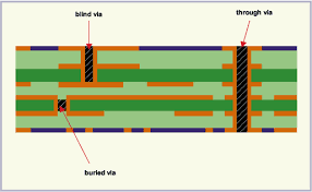
Are Blind Via Holes Suitable For Fine-Pitch Components?
An air bubble in a via can result from any number of things, including drilling the hole too close to an edge of the copper on that layer, not designing the stackup correctly, or manufacturing problems with the laminates used for the PCB. The latter can include issues with the non-uniform weave style of the glass cloths within the laminates (we talked about this in a previous blog).
Another issue that can arise is when a buried via is designed and then drilled to a level below the surface of the copper on the layer where the connection will be made. This can lead to the formation of an X-shaped cavity in the center of the via that will not allow for the necessary contact between the two surfaces of copper and will result in an attenuation of the signal.
There are a few different methods of creating these connections, including controlled depth drilling and laser drilling. Both of these processes have advantages and disadvantages and are typically used when the blind via hole is larger than 6mil. The other option is to use cap construction technology which can be used on smaller blind via holes. This method can save money in the long run but does add to the manufacturing time for the board. In any case, it is important to talk to your PCB manufacturer about their capabilities and what options they offer for these connections.